A little backstory
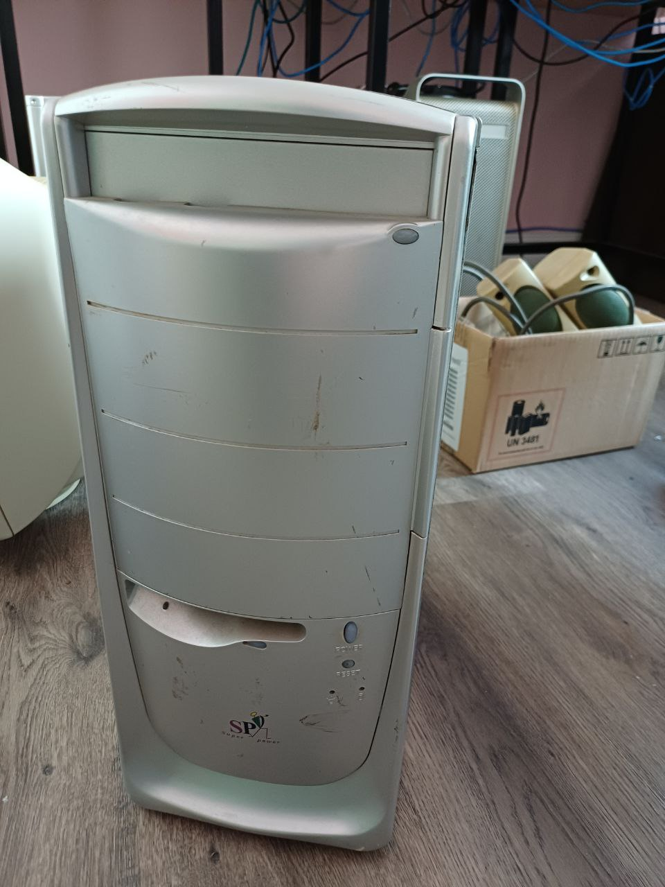
Lately I got a computer from an acquaintance and thought it might not be a big thing. Well it wasn't but ended up being a better computer from what I've expected. It was a Pentium III with both ISA and PCI ports. At first glance it was in a bad condition and horrible mold smell.
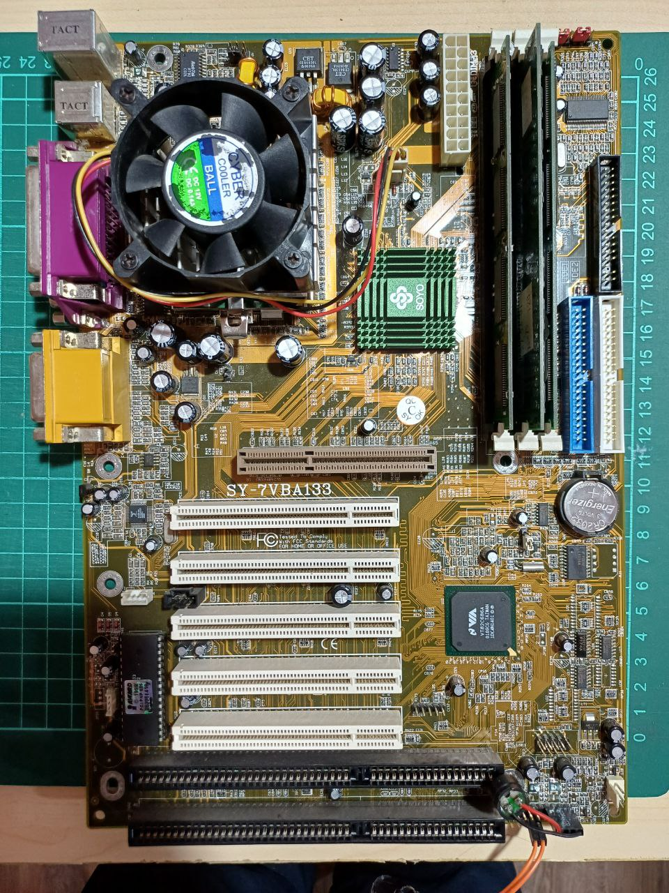
Well and what does this have to do with the flash programmer? This PC has an issue where it can't start from a reboot. Only from a cold boot. This is extremely annoying since every restart means turn the PC off. First I tried replacing capacitors, switching components, etc. but nothing seemed to solve it. My last resort was to try a BIOS update.
Of course that didn't go well. It happened what they always warn it will happen if we aren't caution enough: I messed up the content of the flash. For some reason, both the AWFLASH and UNIFLASH failed on me but that's my fault. I should've done my research better. So here I am with a bad BIOS and some willpower.
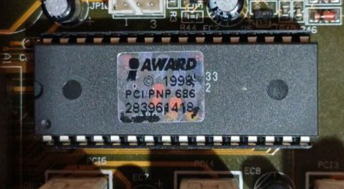
At first glance, the chip doesn't say anything (of course it's behind the sticker).
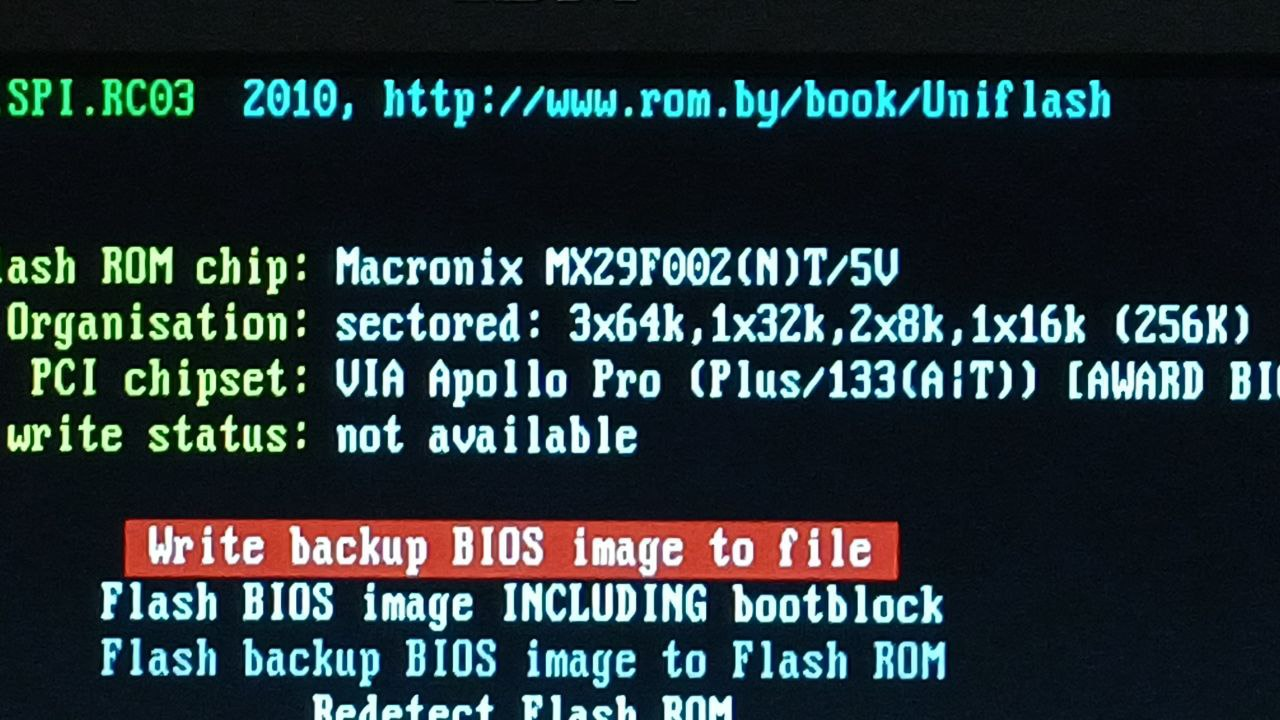
Fortunately for me, I happened to take a picture of the flashing software that identified the chip.
The actual project
At this point I knew I've messed up and decided to check the chip's datasheet. Making a programmer isn't that hard. It's just following the time diagrams and flow charts, a pretty straightforward. First I started researching in case somebody else did it before and I found this article, which not only proved it possible but also set my expectation levels. One of my main worries was the wiring since breadboards and fast signals are not good friends but maybe this was enough. Looking at that design I noticed it used some buffers I didn't have at hand (but I'm keeping the idea, I thought it was neat!). What I did instead is using some shift registers (74HC595) which work as serial to parallel adapters.
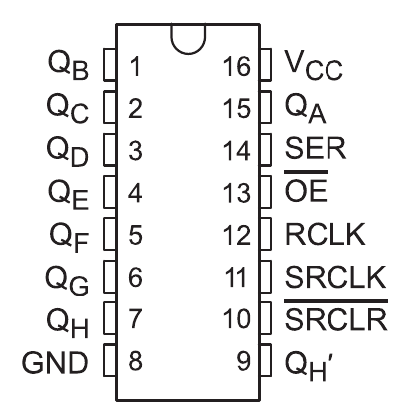
Using the SER input I can send multiple bits and latching them to the Qa through Qh outputs converting 1 bit into 8! Well, kind of. Actually I have to take into account the control lines which are:
- SRCLK: the clock that sends the SER input into the serial buffer
- RCLK: the latch clock that sets the Q bits with whatever there is on the serial buffer
In case this isn't enough, I can chain multiple shift registers using the Qh' output connected to the next SER input and sharing the clocks. I can infinitely extend my one bit data output!
Schematics
At this point I knew this was possible. I only needed a 5V TTL microcontroller and pray for enough pins. The choice in question was the Arduino Nano (actually ATMega328p) which provides with D2 through D13 (excluding serial pins) and A0 through A5 for digital input/outputs. That's a total of... 18 pins. The flash chip has the following pinout:
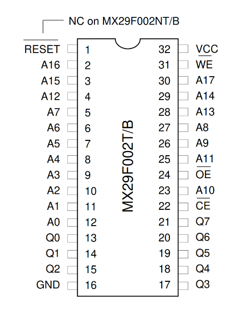
So what I needed was:
- 18 bits for addressing (A0 through A17)
- 8 data pins
- 3 control lines (OE, CE, WE and maybe RESET)
And that's a total of 29-30 pins which is like 10 too many BUT since the address pins are only outputs, I can use shift registers. With two shift registers I reduce a total of 16 pins into 3 which is more than enough. At this point I designed a little circuit which is just a list of connections.
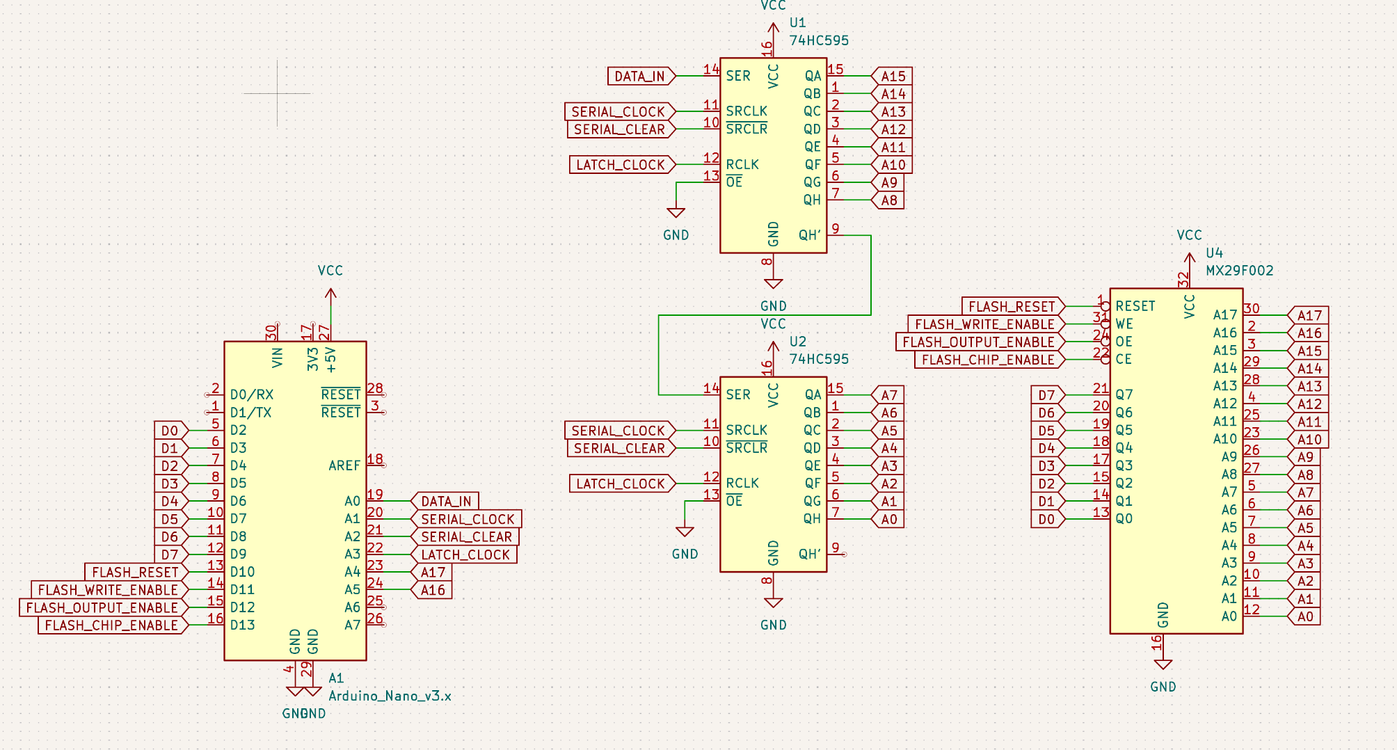
At this point I had every pin connected and a few extra for the control lines I wasn't sure I needed or not. So, in summary:
- D2-D9: data pins Q0-Q8
- D10-D13: control lines
- A0-A3: shift register data and control lines
- A4-A5: the remaining address pins A16 and A17
Wiring everything up (this is when it gets bad)
As I said before, breadboards and fast signals are not good friends but the worst part is also bad connections and hoping I can figure which of the ~40-50 wires is badly connected. The situation looked like this:
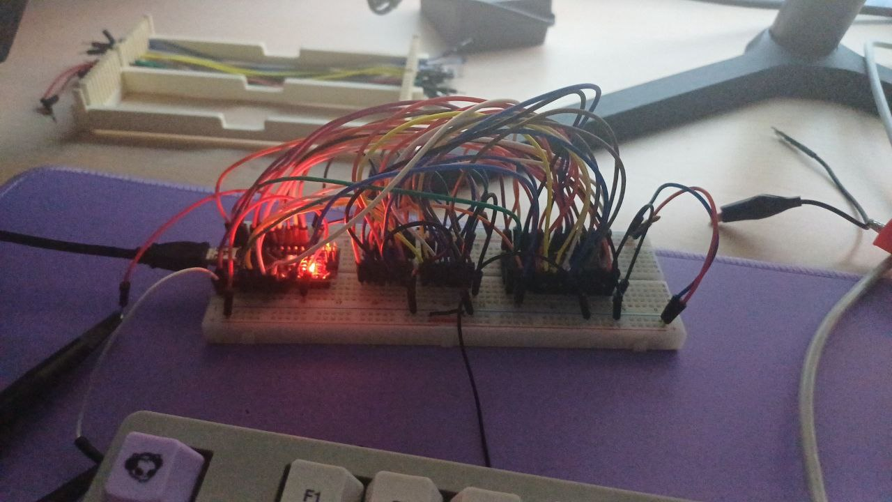
Hard to troubleshoot but I wouldn't make any mistake right? At this point I thought it would be a good idea start coding. Looking at the datasheet there are a bunch of commands but the most important idea is:
- Identifying the chip: this should serve as a simple test to see if the buses are well connected
- Reset command: to restore the chip to a starting state
- Programming an address: which it's pretty cool because once you write an address, the chip answers with the same data byte that was written
- Reading an address: which might help further testing since if I can write an address, I should reliably read it multiple times
- Erasing the flash: I'm still not sure but I think the memory has to be erased in order to program it
Before getting to the programming itself, I should spoil that this didn't work. Initially I thought it was a wiring problem so my next solution was to make a little PCB with the Arduino Nano, the shift registers and sockets for wires:
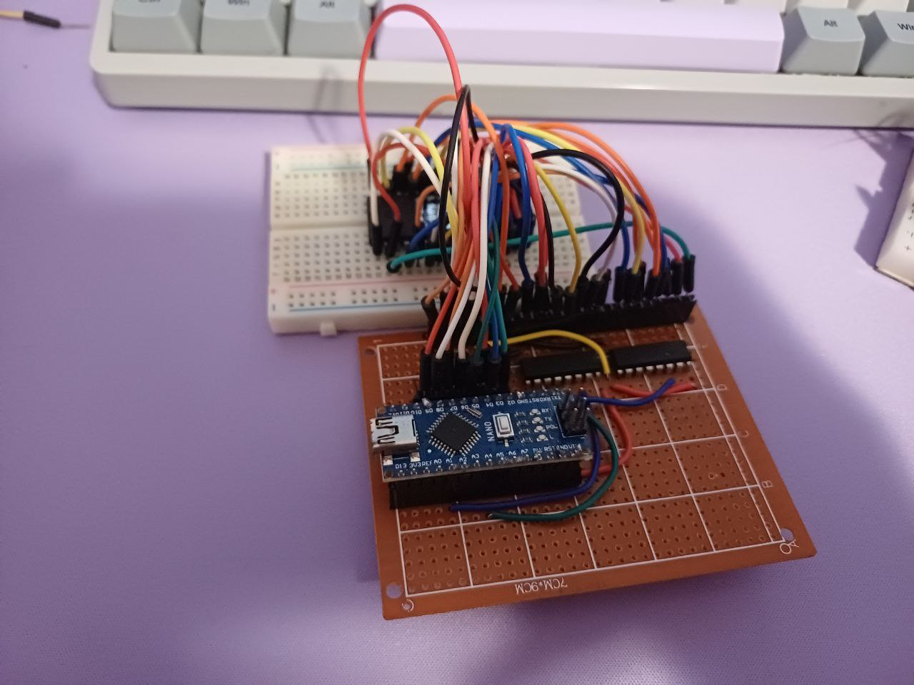
Much better but... this also didn't work! At least not reliably. In both cases, the reads were unstable and some bits flipped. After many hours of testing wire by wire, I found some broken ones and some other bad connections. At this point I thought about giving up. I didn't care that much but at least I could try.
Writing the code (this is when it gets better)
While the programmer didn't do its thing, I still thought the logic I wrote was working fine. First of all, I designed a shift register controller that is quite simple to implement and it's been explained multiple times so I won't talk about it. Then it's simply defining every address pin as output and data pins should alternate between output and input.
The chip works with commands that are basically a series of writes and read at particular addresses. Every write is done after this steps:
- Set the data bus in output mode
- Write the address to the address bus
- Latch the address to the chip by lowering the chip enable and write enable pin
- A byte is set on the data bus
- Latch the data by setting to high the write enable and chip enable pin
This process is described in the datasheet with the typical timings. Since Arduino digitalWrite functions are toooooo slow, no delays are needed. A similar process is done when reading:
- Set the data bas in input mode
- Write the address to the address bus
- Latch the address by lowering the chip enable and output enable pins
- The data byte should be set on the data bus
- After reading the data, set to high the output enable and chip enable pins
Once both functions are implemented, now it's time to test it! The chip identify command consists of the following writes and reads:
- Write to address 0x0555 the 0xAA byte
- Write to address 0x02AA the 0x55 byte
- Write to address 0x0555 the 0x90 byte
- Read the address 0x0000 for the manufacture code (it should be 0xC2)
- Read the address 0x0001 for the device id (it should be 0xB0)
These writes are quite handy because both the addresses and data are made by alternating 0s and 1s. If this command works, it should confirm that the wiring have been done correctly. Except for one little thing. The address alternates 0s and 1s from A0 to A10. I didn't notice this at first. Much much later I saw some weird behavior with A16 and A17 (the ones that weren't outputted by the shift register). I... didn't set them up as outputs. They were floating so the flash chip caught some noise and made it behave erratically. Yeah...
Finally I was ready to implement the main commands. Erase was easy, kind of similar to the chip identification process except it introduces something new: bit toggle. This is the chip's way to tell if a long process is finished or not. While waiting, reading the data bus will flip a bit continuously (that is, every time the output enable pin is lowered). At some point, this process stops and the resulting byte shows a kind of result that we can interpret as done or timeout according to which bit is 1 or 0.
Programming an address is a simple process now: write command, select address and data, wait for toggle pin to stop toggling and if it's done correctly, check the data bus once more to get an echo of the programmed byte in order to verify the process.
And the easiest of them all, reading it's just... set the address and read the data bus.
Once everything was tested and debugged (my test functions are still on the code if you're interested), it's time to write another program that would check the chip, write a bin file and verify its content.
Are we done yet??
No. The cooler idea was to use some protocol like XMODEM to send the data via UART using a serial terminal. As you can imagine, I spent a lot of time with this and felt a little burnt out so I took what I already knew: Python.
The Arduino code expects commands such as read, program, erase and id. The read
and program commands expects 3 bytes for the address and 1 byte for the data.
For example: [0x77][0x00][0x00][0x00][0xAB], where
the first byte is the letter w. The read command just responds with the whole
memory.
Thanks to The Retro Web I got the bios file and could write it using this tool. At this point I felt victorious. Everything showed good signs so writing the image was the last step before the finish line. Right? Almost. A bad habit of myself is that I often forget to think and this was the case. The time estimate of the whole writing process was around two hours!!
What!? How? As I said, I didn't think, I let it run while I was away. Back home,
I see the progress bar stuck at address 0x10000 :D. Back to troubleshooting!
Nah, to make it short I declared a 16 bit int instead of a 32 bit one but
after that smooth sailing! The cause of the slow transfer were the following:
- Slow digital read/writes. Before I decided to use Arduino functions I guessed it was fine but didn't know about the toggle pin which needs many read and writes. Still I don't think this was critical
- Baud rate. I used the typical 115200 baud. Probably could've done it faster
but I wasn't sure how unreliable it will get and at this point I wanted to
finish this. As a reference, sending 0x40000 bytes (every address of the flash
chip) would take:
- 262,144 bytes times 8 bit plus a start and stop bit are 2,621,440 pulses
- And each one of them takes around 9µs (the inverse of the baudrate)
- So that's... 236 seconds of purely data transmission
- My own naivety. Because printing every single byte write in Python surely is free! Reducing the number of prints, reduced the overall time by a nice margin so I accepted that as a solution
Results and conclusions
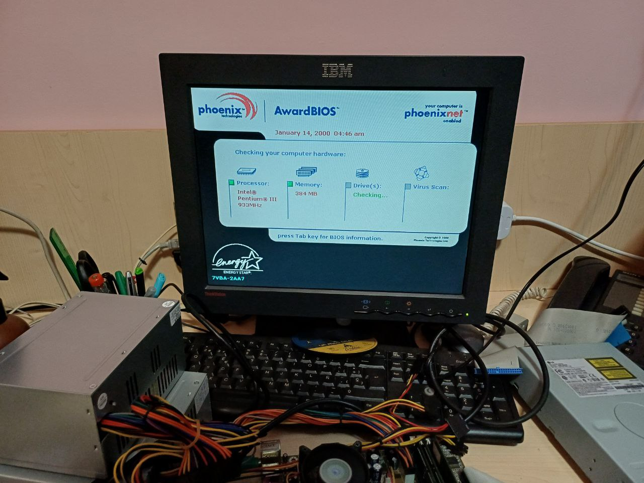
Having done all that, the flash chip tested fine and got my happiest BIOS ever
So this concludes my little project which I expected to finish in two days and finally took like a week. My main takeaway for this projects is that there is no enough checks for silly mistakes. Also thoroughly testing hardware projects is hard. Specially with stuff like this where I wasn't sure what was failing.
In case anyone got here looking for a solution, here's the git repository. I tried to make it as simple and readable as possible. Most of the commands are not implemented since this only cares for programming and reading the chip.
If you got this far, thanks for reading! And if you have good memory you might've been asking if this actually solved the original problem. Of course it didn't! Still this was fun and the PC is still somewhat functional.